- 您现在的位置:买卖IC网 > Sheet目录3879 > PIC18F65J11-I/PT (Microchip Technology)IC PIC MCU FLASH 16KX16 64TQFP
2010 Microchip Technology Inc.
DS39774D-page 139
PIC18F85J11 FAMILY
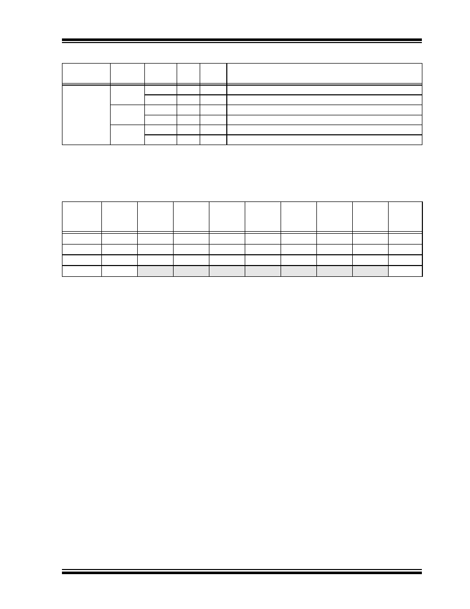
TABLE 11-10: SUMMARY OF REGISTERS ASSOCIATED WITH PORTD
RD7/AD7/PSP7
RD7
0
O
DIG
LATD<7> data output.
1
I
ST
PORTD<7> data input.
AD7(2)
x
O
DIG
External memory interface, address/data bit 7 output.(1)
x
I
TTL
External memory interface, data bit 7 input.(1)
PSP7
x
O
DIG
PSP read output data (LATD<7>); takes priority over port data.
x
I
TTL
PSP write data input.
Name
Bit 7
Bit 6
Bit 5
Bit 4
Bit 3
Bit 2
Bit 1
Bit 0
Reset
Values
on page
PORTD
RD7
RD6
RD5
RD4
RD3
RD2
RD1
RD0
LATD
LATD7
LATD6
LATD5
LATD4
LATD3
LATD2
LATD1
LATD0
TRISD
TRISD7
TRISD6
TRISD5
TRISD4TRISD3TRISD2TRISD1TRISD0
PORTG
RDPU
REPU
RJPU(1)
RG4
RG3
RG2
RG1
RG0
Legend: Shaded cells are not used by PORTD.
Note 1:
Unimplemented on 64-pin devices, read as ‘0’.
TABLE 11-9:
PORTD FUNCTIONS (CONTINUED)
Pin Name
Function
TRIS
Setting
I/O
Type
Description
Legend:
O = Output, I = Input, DIG = Digital Output, ST = Schmitt Buffer Input, TTL = TTL Buffer Input, x = Don’t care (TRIS bit
does not affect port direction or is overridden for this option).
Note 1:
External memory interface I/O takes priority over all other digital and PSP I/O.
2:
Available on 80-pin devices only.
发布紧急采购,3分钟左右您将得到回复。
相关PDF资料
PIC18F2439-E/SO
IC PIC MCU FLASH 6KX16 28SOIC
PIC16LF1938-I/SS
IC MCU 8BIT FLASH 28SSOP
PIC16C621A-20/SO
IC MCU OTP 1KX14 COMP 18SOIC
PIC18F23K22-I/SO
IC PIC MCU 8KB FLASH 28SOIC
PIC18LF2331-I/MM
IC MCU FLASH 4KX16 28QFN
PIC16F639-I/P
IC MCU FLASH 2KX14 20DIP
PIC18F25K20-I/SS
IC PIC MCU FLASH 16KX16 28SSOP
PIC16C58B-04/P
IC MCU OTP 2KX12 18DIP
相关代理商/技术参数
PIC18F65J11T-I/PT
功能描述:8位微控制器 -MCU 32KB Flash 2048bytes-RAM 51I/O RoHS:否 制造商:Silicon Labs 核心:8051 处理器系列:C8051F39x 数据总线宽度:8 bit 最大时钟频率:50 MHz 程序存储器大小:16 KB 数据 RAM 大小:1 KB 片上 ADC:Yes 工作电源电压:1.8 V to 3.6 V 工作温度范围:- 40 C to + 105 C 封装 / 箱体:QFN-20 安装风格:SMD/SMT
PIC18F65J15-I/PT
功能描述:8位微控制器 -MCU 32 KB FL 2KB RAM RoHS:否 制造商:Silicon Labs 核心:8051 处理器系列:C8051F39x 数据总线宽度:8 bit 最大时钟频率:50 MHz 程序存储器大小:16 KB 数据 RAM 大小:1 KB 片上 ADC:Yes 工作电源电压:1.8 V to 3.6 V 工作温度范围:- 40 C to + 105 C 封装 / 箱体:QFN-20 安装风格:SMD/SMT
PIC18F65J15T-I/PT
功能描述:8位微控制器 -MCU 32 KB FL 2KB RAM RoHS:否 制造商:Silicon Labs 核心:8051 处理器系列:C8051F39x 数据总线宽度:8 bit 最大时钟频率:50 MHz 程序存储器大小:16 KB 数据 RAM 大小:1 KB 片上 ADC:Yes 工作电源电压:1.8 V to 3.6 V 工作温度范围:- 40 C to + 105 C 封装 / 箱体:QFN-20 安装风格:SMD/SMT
PIC18F65J50-I/PT
功能描述:8位微控制器 -MCU 32KB FLSH 3936Bs RAM USB 2.0 nanoWatt RoHS:否 制造商:Silicon Labs 核心:8051 处理器系列:C8051F39x 数据总线宽度:8 bit 最大时钟频率:50 MHz 程序存储器大小:16 KB 数据 RAM 大小:1 KB 片上 ADC:Yes 工作电源电压:1.8 V to 3.6 V 工作温度范围:- 40 C to + 105 C 封装 / 箱体:QFN-20 安装风格:SMD/SMT
PIC18F65J50T-I/PT
功能描述:8位微控制器 -MCU 32KB FLSH 3936Bs RAM USB 2.0 nanoWatt RoHS:否 制造商:Silicon Labs 核心:8051 处理器系列:C8051F39x 数据总线宽度:8 bit 最大时钟频率:50 MHz 程序存储器大小:16 KB 数据 RAM 大小:1 KB 片上 ADC:Yes 工作电源电压:1.8 V to 3.6 V 工作温度范围:- 40 C to + 105 C 封装 / 箱体:QFN-20 安装风格:SMD/SMT
PIC18F65J90-I/PT
功能描述:8位微控制器 -MCU 32KB FL 2048b RAM 51I/O 8b Fam RoHS:否 制造商:Silicon Labs 核心:8051 处理器系列:C8051F39x 数据总线宽度:8 bit 最大时钟频率:50 MHz 程序存储器大小:16 KB 数据 RAM 大小:1 KB 片上 ADC:Yes 工作电源电压:1.8 V to 3.6 V 工作温度范围:- 40 C to + 105 C 封装 / 箱体:QFN-20 安装风格:SMD/SMT
PIC18F65J90-I/PT
制造商:Microchip Technology Inc 功能描述:IC MCU 8BIT 32K FLASH SMD TQFP64
PIC18F65J90T-I/PT
功能描述:8位微控制器 -MCU 32KB Flash 2048bytes-RAM 51I/O RoHS:否 制造商:Silicon Labs 核心:8051 处理器系列:C8051F39x 数据总线宽度:8 bit 最大时钟频率:50 MHz 程序存储器大小:16 KB 数据 RAM 大小:1 KB 片上 ADC:Yes 工作电源电压:1.8 V to 3.6 V 工作温度范围:- 40 C to + 105 C 封装 / 箱体:QFN-20 安装风格:SMD/SMT